
Introduction to Logic Families:
Logic Gates like NAND, NOR are used in daily applications for performing logic operations. The Gates are manufactured using semiconductor devices like BJT, Diodes, or FETs. Different Gate’s are constructed using Integrated circuits. Digital logic circuits are manufactured depending on the specific circuit technology or logic families.
The different logic families are:
- RTL(Resistor Transistor Logic)
- DTL(Diode Transistor Logic)
- TTL(Transistor-Transistor Logic)
- ECL(Emitter Coupled Logic)
- CMOS(Complementary Metal Oxide Semiconductor Logic)
Features of Logic Families:
- Fan Out: Number of loads the output of a GATE can drive without effecting its usual performance. By load we mean the amount of current required by the input of another Gate connected to the output of the given gate.
- Power Dissipation: It represents the amount of power needed by the device. It is measured in mW. It is usually the product of supply voltage and the amount of average current drawn when the output is high or low.
- Propagation Delay: It represents the transition time which elapses when the input level changes. The delay which occurs for the output to make its transition is the propagation delay.
- Noise Margin: It represents the amount of noise voltage allowed at the input, which doesn’t affect the standard output.
Introduction to TTLs:
It is a logical family consisting completely of transistors. It employs a transistor with multiple emitters. Commercially it starts with the 74 series like the 7404, 74S86, etc. It was built in 1961 by James L Bui and commercially used in logic design in 1963
Classification of TTL:
TTLs are classified based on the output.
1. Open Collector Output: The main feature is that its output is 0 when low and floating when high. Usually, an external Vcc may be applied.
RTL
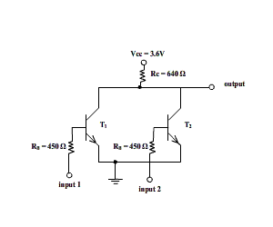
The resistor-transistor logic, also termed as RTL, was most popular kind of logic before the invention of IC fabrication technologies.
As its name suggests, RTL circuits mainly consists of resistors and transistors that comprises RTL devices.
The basic RTL device is a NOR gate, shown in figure aside.
Inputs to the NOR gate shown above are ‘input1’ & ‘input2’. The inputs applied at these terminals represent either logic level HIGH (1) or LOW (0).
The logic level LOW is the voltage that drives corresponding transistor in cut-off region, while logic level HIGH drives it into saturation region.
If both the inputs are LOW, then both the transistors are in cut-off i.e. they are turned-off. Thus, voltage Vcc appears at output I.e. HIGH.
If either transistor or both of them are applied HIGH input, the voltage Vcc drops across Rc and output is LOW.
RTL family is characterized by poor noise margin, poor fan-out capability, low speed and high power dissipation. Due to these undesirable characteristics, this family is now obsolete.
Diode-Transistor Logic (DTL) family
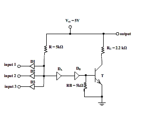
The diode-transistor logic, also termed as DTL, replaced RTL family because of greater fan-out capability and more noise margin.
As its name suggests, DTL circuits mainly consists of diodes and transistors that comprises DTL devices.
The basic DTL device is a NAND gate, shown aside.
Three inputs to the gate are applied through three diodes viz. D1, D2 and D3. The diode will conduct only when corresponding input is LOW.
If any of the diode is conducting i.e. when at least one input is LOW, the voltage at cathode of didoe DA is such that it keeps transistor T in cut-off and subsequently, output of transistor is HIGH.
If all inputs are HIGH, all diodes are non-conducting, transistor T is in saturation, and its output is LOW.
Due to number of diodes used in this circuit, the speed of the circuit is significantly low. Hence this family of logic gates is modified to transistor-transistor logic i.e. TTL family.
Transistor-Transistor Logic (TTL) family
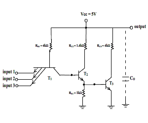
TTL family is a modification to the DTL. It has come to existence so as to overcome the speed limitations of DTL family. The basic gate of this family is TTL NAND gate.
Modifications to DTL NAND-
1. The diodes D1, D2 and D3 are replaced by emitter-base junctions of a multiple-emitter transistor labeled T1.
2. Diode DA is replaced by collector-base junction of T1.
3. Diode DB is replaced by emitter-base junction of transistor labeled T2.
The working of this circuit is identical to that of DTL circuit.
Case1- When at least one input is logic LOW, transistor T2 and T3 are in cut-off and hence, output of T3 is HIGH.
Case2- When all inputs are HIGH, T1 operates in active inverse mode, driving T2 & T3 in saturation. Since T3 is ON, the output is LOW.
Case3- While all inputs are HIGH, if any of the inputs suddenly goes LOW, then T2 and T3 will be turned off only when stored base charge is removed. The collector-base junction of T1 is back-biased and T1 operates in normal active region. A large collector current of T1 is in such direction that it helps removing base charge of T2 and T3. In this way, the circuit speed is increased in TTL over speed of DTL.
Emitter Coupled Logic (ECL) family
ECL logic family implements the gates in differential amplifier configuration in which transistors are never driven in the saturation region thereby improving the speed of circuit to a great extent. The ECL family is fastest of all logic families.
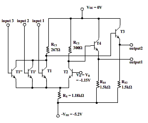
The basic gate of ECL family is NOR gate (OR and NOR together) as shown in diagram. The output1 is OR output while ouput2 is NOR output.
Transistor T1 is applied with input and additional inputs are applied to transistors (T1’, T1’’, . . .) in parallel with T1. Thus transistor(s) T1 and T2 are connected in differential amplifier configuration.
Transistors T3 and T4 are emitter-followers used for DC level-shifting of output voltages.
The positive supply terminal of the circuit is grounded while negative supply terminal is at negative 5.2V. This is done to minimize the effect of noise introduced by the power supply and also to protect the gate from short-circuit that might occur accidently.
Both the outputs (HIGH/LOW) for OR and NOR are negative. Thus, to interface this logic family with other, a translator circuit is needed which converts negative voltages to compatible positive voltage levels.
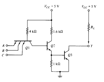
MOS Logic family
MOS logic family implements the logic gates using MOSFET devices. MOSFETs are high density devices which can easily and economically fabricated on ICs. MOS logic gates can be fabricated using either only NMOS or only PMOS devices.
MOS logic is vastly used in LSI and VLSI devices, such as microprocessor chips, due to their high density characteristic.
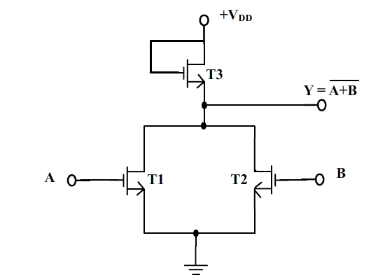
NMOS NOR gate is shown in figure.
If both transistors T1 and T2 are off i.e. A = B = LOW, then output is HIGH = VDD.
If either of the inputs is HIGH, then corresponding transistor(s) is/are ON, thus connecting output to GND i.e. LOW.
MOS logic is vastly used in LSI and VLSI devices, such as microprocessor chips, due to their high density characteristic.
NMOS NOR gate is shown in figure.
If both transistors T1 and T2 are off i.e. A = B = LOW, then output is HIGH = VDD.
If either of the inputs is HIGH, then corresponding transistor(s) is/are ON, thus connecting output to GND i.e. LOW.
If both inputs are ON, then only both T1 and T2 are ON and output is LOW; otherwise (when either or both transistors are OFF,) the output is HIGH.
This is NAND operation on applied inputs.
!! Caution for using MOS devices:
If any of input of MOS is left unconnected, the open input terminal which has very high input impedance may take any stray electric charge as input and can develop extreme dangerous high voltage which can damage the device and may also harm the person handling the device.
Thus, none of the un-used inputs of MOS device should be left unconnected. It must connected to ground or supply. Even for storage of device, all pins must be shorted.
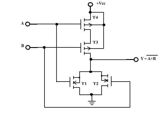
CMOS Logic family
CMOS stands for complementary-MOS, in which both p-channel and n-channel enhancement MOSFET devices are fabricated on same chip. This causes density to be reduced and complex fabrication process. However, CMOS devices consume negligible power and hence are preferred over MOS devices in battery operated applications.
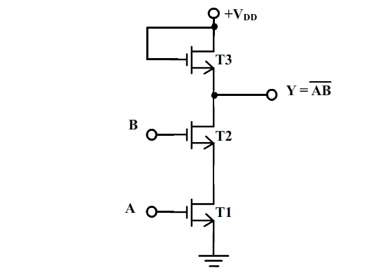
A CMOS NAND gate is shown in figure aside.
T1 and T2 are n-channel MOSFETs while T3 and T4 are p-channel MOSFETs.
When both inputs A & B are HIGH, then T1 & T2 are ON while T3 & T4 are OFF. Hence, output is connected to GND i.e. LOW.
If either input is LOW, then either T3 or T4 is ON, connecting output is +Vcc i.e. HIGH.
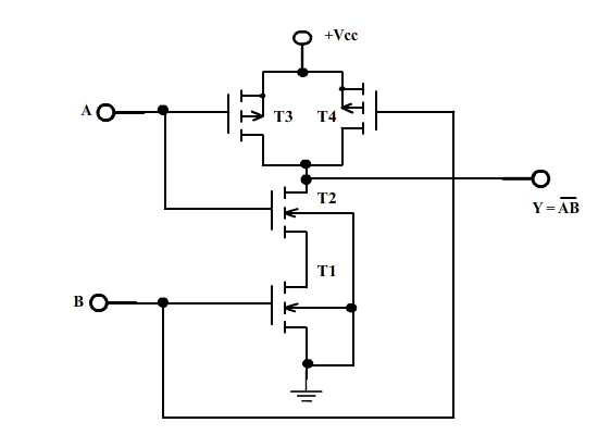
Similar is working of CMOS NOR gate shown in figure aside. Here, p-channel devices are in series and n-channel devices are in parallel.
No comments:
Post a Comment