
REGISTERS
We know that one flip-flop can store one-bit of information. In order to store multiple bits of information, we require multiple flip-flops. The group of flip-flops, which are used to hold the binary data is known as register.
Shift Registers in Digital Logic
The information stored within these registers can be transferred with the help of shift registers. Shift Register is a group of flip flops used to store multiple bits of data. The bits stored in such registers can be made to move within the registers and in/out of the registers by applying clock pulses. An n-bit shift register can be formed by connecting n flip-flops where each flip flop stores a single bit of data.
If the register is capable of shifting bits either towards right hand side or towards left hand side is known as shift register. An ‘N’ bit shift register contains ‘N’ flip-flops.
The registers which will shift the bits to left are called “Shift left registers”.
The registers which will shift the bits to right are called “Shift right registers”.
The registers which will shift the bits to right are called “Shift right registers”.
Shift registers are basically of 4 types. These are:
- Serial In Serial Out shift register
- Serial In parallel Out shift register
- Parallel In Serial Out shift register
- Parallel In parallel Out shift register
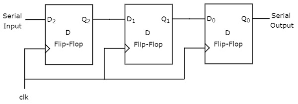
Serial-In Serial-Out Shift Register (SISO) –
The shift register, which allows serial input (one bit after the other through a single data line) and produces a serial output is known as Serial-In Serial-Out shift register. Since there is only one output, the data leaves the shift register one bit at a time in a serial pattern, thus the name Serial-In Serial-Out Shift Register.
The logic circuit given below shows a serial-in serial-out shift register. The circuit consists of four D flip-flops which are connected in a serial manner. All these flip-flops are synchronous with each other since the same clock signal is applied to each flip flop.
In this shift register, we can send the bits serially from the input of left most D flip-flop. Hence, this input is also called as serial input. For every positive edge triggering of clock signal, the data shifts from one stage to the next. So, we can receive the bits serially from the output of right most D flip-flop. Hence, this output is also called as serial output.
Serial-In Parallel-Out shift Register (SIPO) –
The shift register, which allows serial input (one bit after the other through a single data line) and produces a parallel output is known as Serial-In Parallel-Out shift register.
The logic circuit given below shows a serial-in-parallel-out shift register. The circuit consists of four D flip-flops which are connected. The clear (CLR) signal is connected in addition to the clock signal to all the 4 flip flops in order to RESET them. The output of the first flip flop is connected to the input of the next flip flop and so on. All these flip-flops are synchronous with each other since the same clock signal is applied to each flip flop.
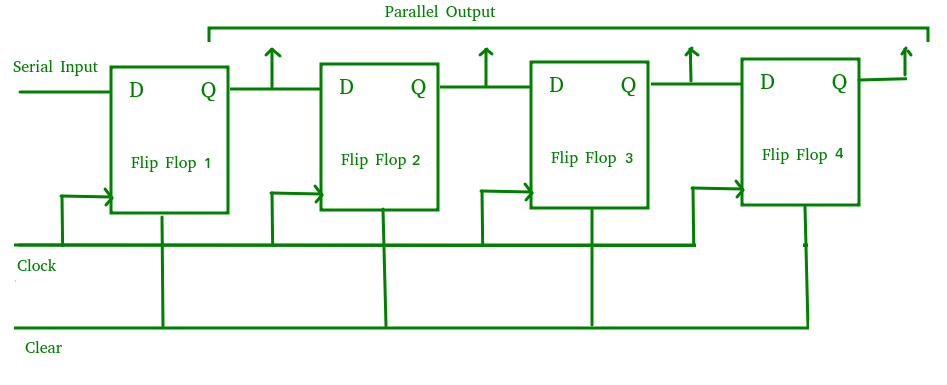
The above circuit is an example of shift right register, taking the serial data input from the left side of the flip flop and producing a parallel output. They are used in communication lines where demultiplexing of a data line into several parallel lines is required because the main use of the SIPO register is to convert serial data into parallel data.
Parallel-In Serial-Out Shift Register (PISO) –
The shift register, which allows parallel input (data is given separately to each flip flop and in a simultaneous manner) and produces a serial output is known as Parallel-In Serial-Out shift register.
The logic circuit given below shows a parallel-in-serial-out shift register. The circuit consists of four D flip-flops which are connected. The clock input is directly connected to all the flip flops but the input data is connected individually to each flip flop through a multiplexer at the input of every flip flop. The output of the previous flip flop and parallel data input are connected to the input of the MUX and the output of MUX is connected to the next flip flop. All these flip-flops are synchronous with each other since the same clock signal is applied to each flip flop.
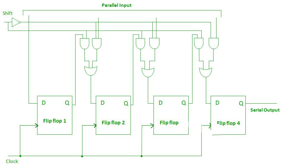
A Parallel in Serial out (PISO) shift register us used to convert parallel data to serial data.
Parallel-In Parallel-Out Shift Register (PIPO) –
The shift register, which allows parallel input (data is given separately to each flip flop and in a simultaneous manner) and also produces a parallel output is known as Parallel-In parallel-Out shift register.
The logic circuit given below shows a parallel-in-parallel-out shift register. The circuit consists of four D flip-flops which are connected. The clear (CLR) signal and clock signals are connected to all the 4 flip flops. In this type of register, there are no interconnections between the individual flip-flops since no serial shifting of the data is required. Data is given as input separately for each flip flop and in the same way, output also collected individually from each flip flop.
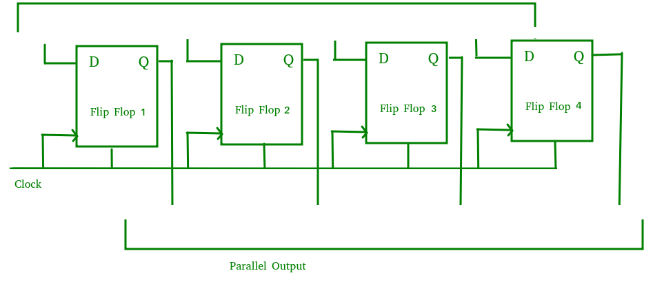
A Parallel in Parallel out (PIPO) shift register is used as a temporary storage device and like SISO Shift register it acts as a delay element.
No comments:
Post a Comment